JOURNEY THROUGH THESilicon World
Wrocław Tech and TU Graz students explore the world of semiconductors in a Unite! Seed Fund project that combines education, hands-on experience and international exchange.
It starts with sand...
Common sand contains a lot of silicon dioxide (SiO₂). But it's not pure enough for electronics. The journey begins by extracting and refining silicon from quartz sand through a high-temperature chemical process - a requirement for creating reliable microchips.
Purifying the Sand
Silicon sand contains a lot of silicon dioxide (SiO₂). The journey begins by extracting and refining silicon from quartz sand through a high-temperature process - a requirement for creating reliable microchips. Silicon is purified to 99.9999999% (nine nines) purity.
Growing a Silicon Ingot
The ultra-pure silicon is melted and grown into a single large crystal using a process called the Czochralski method. A seed is shaped into a cylindrical ingot - a perfect silicon structure that forms the base for every modern microchip.
Wafer Slicing and Polishing
The silicon ingot is sliced into thin wafers, like microscopic pancakes. Each wafer is polished to atomic-level smoothness, creating a flat surface ready for circuit printing. These wafers are now ready for microchip design.
Circuit Printing
Photolithography transfers the circuit pattern onto the wafer using light. Layer by layer, transistors are built at nanometer scale - smaller than a virus. A single modern chip contains billions of transistors.
Packaging & Testing
Each chip is cut from the wafer, tested for defects, and packaged into the familiar black chips we know. From raw sand to finished processor - the journey of silicon is complete.
The EU Chips Act
In 2023, the European Union passed the EU Chips Act - a landmark regulation to secure Europe's semiconductor supply chain, reduce strategic dependencies, and make Europe a global leader in chip technology by 2030.
Our project embraced this ambition directly - bringing engineering students face-to-face with chip fabs, clean rooms, and research labs to broaden awareness of semiconductors as a strategic industry.
€43B
in public and private investment mobilised by 2030
20%
target share of global chip production - up from ~9% today
2030
target year for doubling Europe's share of world chip output
~9%
Europe's current share of global semiconductor production
Source: European Commission — EU Chips Act, 2023
The Exchange
Two student communities. Two countries. One shared passion for technology.
May 2025
Graz, Austria
Members of KN Solvro visited Graz - the Silicon Valley of Europe. They toured ams OSRAM's production facilities including a Clean Room, explored Silicon Austria Labs' cutting-edge research, and visited laboratories at Technische Universität Graz. The Austrian students from BEST Graz ensured the visit combined technical depth with cultural warmth.
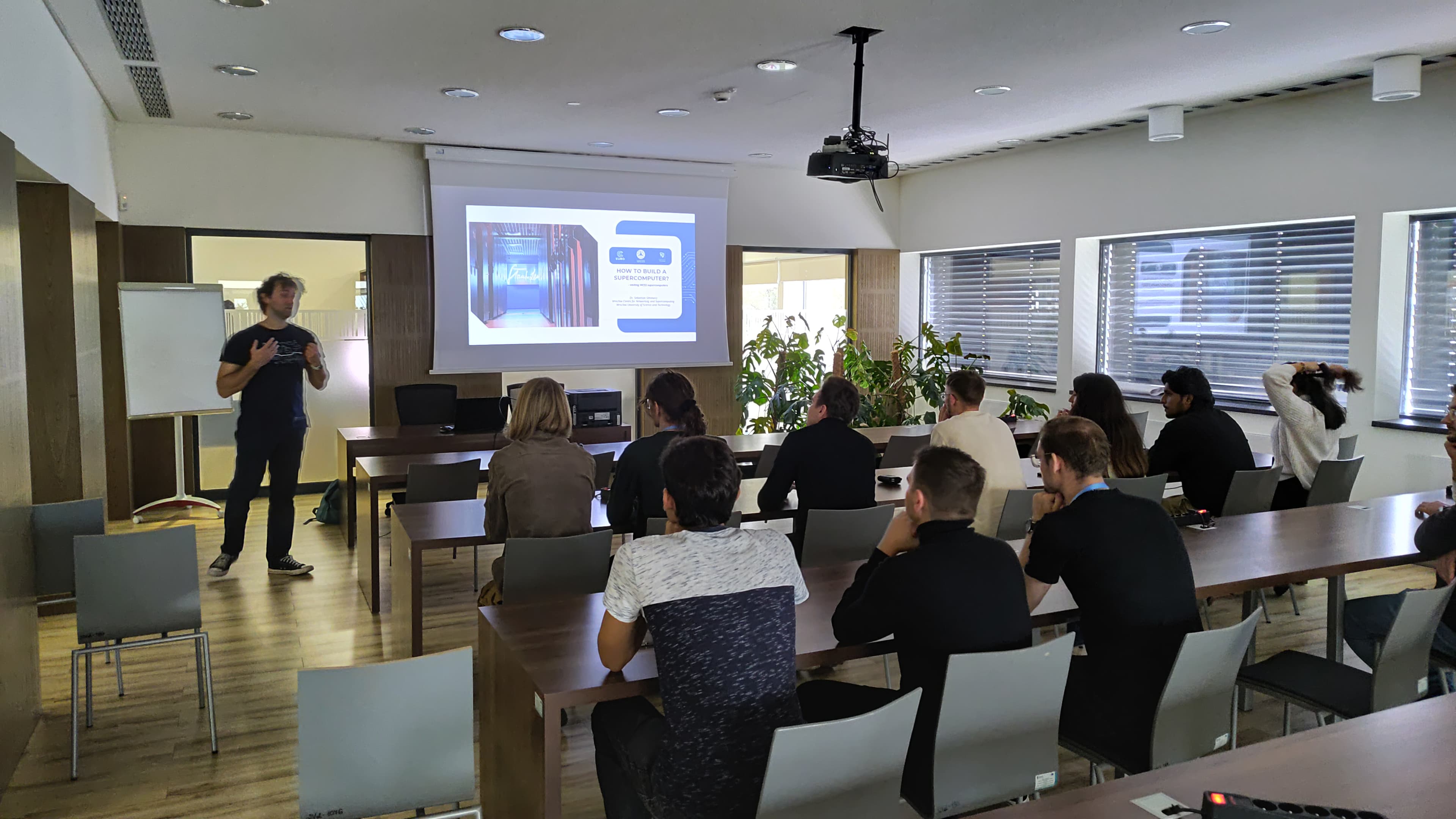
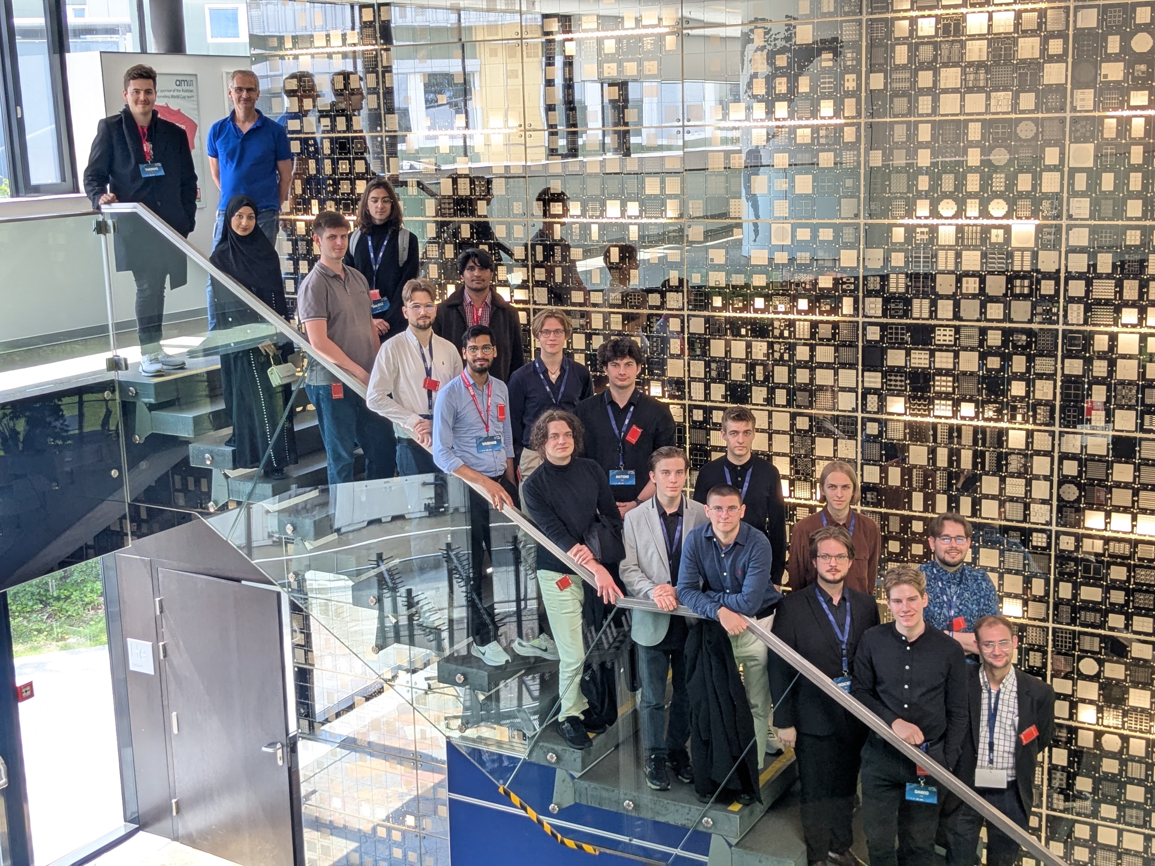
October 2025
Wrocław, Poland
TU Graz students visited Wrocław, hosted by KN Solvro. They explored XTPL's nanoprinting technology, Balluff's sensor solutions, and the Wrocław Centre for Networking and Supercomputing (WCSS). The programme also included a tour of the Faculty of Electronics at Wrocław Tech, including the specialist Clean Room, organized with the NaMi student research group.
Organizers
The two student organisations behind the project.

The biggest IT student organization of its kind in Poland. Based at WUST, but with international impact - we build apps from students to students, push the boundaries of science through AI/ML research, and foster community by running events that empower the next generation of skilled engineers.

A student organisation at TU Graz with 20 active members, dedicated to connecting students with industry and academia through international events and career fairs.
Funded by

In cooperation with